- 您现在的位置:买卖IC网 > Sheet目录3889 > PIC16F873T-04E/SO (Microchip Technology)IC MCU FLASH 4KX14 EE 28SOIC
2001 Microchip Technology Inc.
DS30292C-page 73
PIC16F87X
9.2
MSSP I2C Operation
The MSSP module in I2C mode, fully implements all
master and slave functions (including general call sup-
port) and provides interrupts on START and STOP bits in
hardware, to determine a free bus (multi-master func-
tion). The MSSP module implements the standard mode
specifications, as well as 7-bit and 10-bit addressing.
Refer to Application Note AN578, "Use of the SSP
Module in the I 2C Multi-Master Environment."
A "glitch" filter is on the SCL and SDA pins when the pin
is an input. This filter operates in both the 100 kHz and
400 kHz modes. In the 100 kHz mode, when these pins
are an output, there is a slew rate control of the pin that
is independent of device frequency.
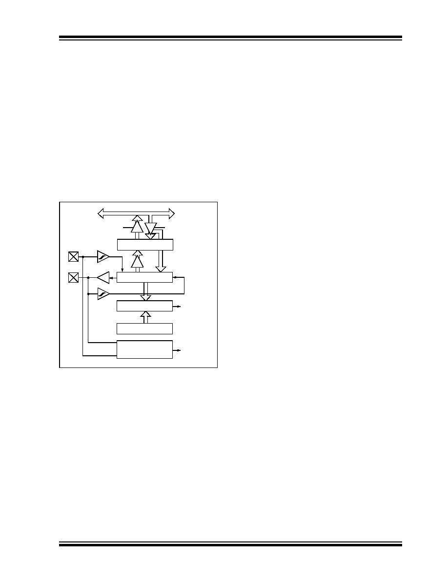
FIGURE 9-5:
I2C SLAVE MODE BLOCK
DIAGRAM
Two pins are used for data transfer. These are the SCL
pin, which is the clock, and the SDA pin, which is the
data. The SDA and SCL pins are automatically config-
ured when the I2C mode is enabled. The SSP module
functions are enabled by setting SSP Enable bit
SSPEN (SSPCON<5>).
The MSSP module has six registers for I2C operation.
They are the:
SSP Control Register (SSPCON)
SSP Control Register2 (SSPCON2)
SSP Status Register (SSPSTAT)
Serial Receive/Transmit Buffer (SSPBUF)
SSP Shift Register (SSPSR) - Not directly
accessible
SSP Address Register (SSPADD)
The SSPCON register allows control of the I2C opera-
tion. Four mode selection bits (SSPCON<3:0>) allow
one of the following I2C modes to be selected:
I2C Slave mode (7-bit address)
I2C Slave mode (10-bit address)
I2C Master mode, clock = OSC/4 (SSPADD +1)
I2C firmware modes (provided for compatibility to
other mid-range products)
Before selecting any I2C mode, the SCL and SDA pins
must be programmed to inputs by setting the appropri-
ate TRIS bits. Selecting an I2C mode by setting the
SSPEN bit, enables the SCL and SDA pins to be used
as the clock and data lines in I2C mode. Pull-up resis-
tors must be provided externally to the SCL and SDA
pins for the proper operation of the I2C module.
The CKE bit (SSPSTAT<6:7>) sets the levels of the
SDA and SCL pins in either Master or Slave mode.
When CKE = 1, the levels will conform to the SMBus
specification. When CKE = 0, the levels will conform to
the I2C specification.
The SSPSTAT register gives the status of the data
transfer. This information includes detection of a
START (S) or STOP (P) bit, specifies if the received
byte was data or address, if the next byte is the com-
pletion of 10-bit address, and if this will be a read or
write data transfer.
SSPBUF is the register to which the transfer data is
written to, or read from. The SSPSR register shifts the
data in or out of the device. In receive operations, the
SSPBUF and SSPSR create a doubled buffered
receiver. This allows reception of the next byte to begin
before reading the last byte of received data. When the
complete byte is received, it is transferred to the
SSPBUF register and flag bit SSPIF is set. If another
complete byte is received before the SSPBUF register
is read, a receiver overflow has occurred and bit
SSPOV (SSPCON<6>) is set and the byte in the
SSPSR is lost.
The SSPADD register holds the slave address. In
10-bit mode, the user needs to write the high byte of the
address (1111 0 A9 A8 0). Following the high byte
address match, the low byte of the address needs to be
loaded (A7:A0).
Read
Write
SSPSR Reg
Match Detect
SSPADD Reg
START and
STOP bit Detect
SSPBUF Reg
Internal
Data Bus
Addr Match
Set, Reset
S, P bits
(SSPSTAT Reg)
SCL
Shift
Clock
MSb
LSb
SDA
发布紧急采购,3分钟左右您将得到回复。
相关PDF资料
PIC16F877T-10E/PT
IC MCU FLASH 8KX14 EE 44TQFP
22-15-3053
CONN FFC/FPC 5POS .100 RT ANG
PIC16C58BT-40/SS
IC MCU OTP 2KX12 20SSOP
PIC16C57CT-40/SO
IC MCU OTP 2KX12 28SOIC
PIC16C55AT-40/SO
IC MCU OTP 512X12 28SOIC
PIC16C56AT-40/SO
IC MCU OTP 1KX12 18SOIC
PIC16C57CT-40/SS
IC MCU OTP 2KX12 28SSOP
22-02-3053
CONN FFC/FPC 5POS .100 VERTICAL
相关代理商/技术参数
PIC16F873T-04I/SO
功能描述:8位微控制器 -MCU 7KB 192 RAM 22 I/O RoHS:否 制造商:Silicon Labs 核心:8051 处理器系列:C8051F39x 数据总线宽度:8 bit 最大时钟频率:50 MHz 程序存储器大小:16 KB 数据 RAM 大小:1 KB 片上 ADC:Yes 工作电源电压:1.8 V to 3.6 V 工作温度范围:- 40 C to + 105 C 封装 / 箱体:QFN-20 安装风格:SMD/SMT
PIC16F873T-10E/SO
功能描述:8位微控制器 -MCU 7KB 192 RAM 22 I/O RoHS:否 制造商:Silicon Labs 核心:8051 处理器系列:C8051F39x 数据总线宽度:8 bit 最大时钟频率:50 MHz 程序存储器大小:16 KB 数据 RAM 大小:1 KB 片上 ADC:Yes 工作电源电压:1.8 V to 3.6 V 工作温度范围:- 40 C to + 105 C 封装 / 箱体:QFN-20 安装风格:SMD/SMT
PIC16F873T-20/SO
功能描述:8位微控制器 -MCU 7KB 192 RAM 22 I/O RoHS:否 制造商:Silicon Labs 核心:8051 处理器系列:C8051F39x 数据总线宽度:8 bit 最大时钟频率:50 MHz 程序存储器大小:16 KB 数据 RAM 大小:1 KB 片上 ADC:Yes 工作电源电压:1.8 V to 3.6 V 工作温度范围:- 40 C to + 105 C 封装 / 箱体:QFN-20 安装风格:SMD/SMT
PIC16F873T-20I/SO
功能描述:8位微控制器 -MCU 7KB 192 RAM 22 I/O RoHS:否 制造商:Silicon Labs 核心:8051 处理器系列:C8051F39x 数据总线宽度:8 bit 最大时钟频率:50 MHz 程序存储器大小:16 KB 数据 RAM 大小:1 KB 片上 ADC:Yes 工作电源电压:1.8 V to 3.6 V 工作温度范围:- 40 C to + 105 C 封装 / 箱体:QFN-20 安装风格:SMD/SMT
PIC16F874-04/L
功能描述:8位微控制器 -MCU 7KB 192 RAM 33 I/O RoHS:否 制造商:Silicon Labs 核心:8051 处理器系列:C8051F39x 数据总线宽度:8 bit 最大时钟频率:50 MHz 程序存储器大小:16 KB 数据 RAM 大小:1 KB 片上 ADC:Yes 工作电源电压:1.8 V to 3.6 V 工作温度范围:- 40 C to + 105 C 封装 / 箱体:QFN-20 安装风格:SMD/SMT
PIC16F874-04/L
制造商:Microchip Technology Inc 功能描述:8BIT FLASH MCU SMD 16F874 PLCC44
PIC16F87404/P
制造商:Microchip Technology Inc 功能描述:MICROCONTROLLER IC
PIC16F874-04/P
功能描述:8位微控制器 -MCU 7KB 192 RAM 33 I/O RoHS:否 制造商:Silicon Labs 核心:8051 处理器系列:C8051F39x 数据总线宽度:8 bit 最大时钟频率:50 MHz 程序存储器大小:16 KB 数据 RAM 大小:1 KB 片上 ADC:Yes 工作电源电压:1.8 V to 3.6 V 工作温度范围:- 40 C to + 105 C 封装 / 箱体:QFN-20 安装风格:SMD/SMT